Guidelines for Semicon 2.0 scheme notified: How it affects businesses
What's the story
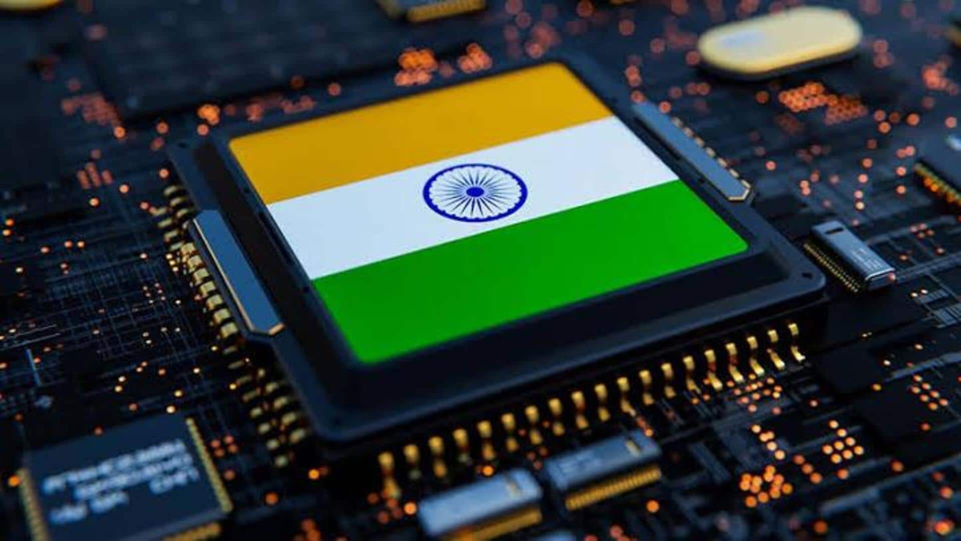
The Indian government has notified the detailed framework for its Semicon 2.0 scheme, which aims to boost the country's semiconductor ecosystem. The scheme will provide fiscal support across six key pillars: chip design, fabrication (fabs), advanced packaging, semiconductor equipment and materials, research and development (R&D), and talent development. The Ministry of Electronics and Information Technology (MeitY) issued the notification today.
Financial backing
Support for silicon semiconductor wafer fabs
Under Semicon 2.0, the government will provide 40% fiscal support for silicon semiconductor wafer fabs.
For advanced packaging technologies such as 2.5D and 3D packaging, wafer-level chip-scale packaging, and heterogeneous integration, the government will give 35% of eligible capital expenditure on a pari-passu basis.
Legacy packaging projects will get a lower support of 25%.
Investment goals
Semicon 2.0 scheme expected to run for 6 years
The Semicon 2.0 scheme is expected to run for six years, with an initial application window of three years.
The India Semiconductor Mission (ISM) will be the nodal agency for implementing this scheme.
The government's Cabinet presentation had projected around ₹4 lakh crore in investment from the program, ₹2 lakh crore in production and ₹1 lakh crore in exports.
Research funding
Support for advanced semiconductor R&D
The new Semicon 2.0 scheme also includes support for advanced semiconductor research and development (R&D). This covers the CMOS process technologies, silicon photonics, display fabrication, as well as chiplet-based packaging.